


TLDR: Recent advancements in metasurfaces enhance the performance of 2D materials by improving their optical properties through etching. This technique boosts efficiency in electronic devices, paving the way for innovative applications in telecommunications and energy harvesting, and signifies a promising future in material science and engineering.
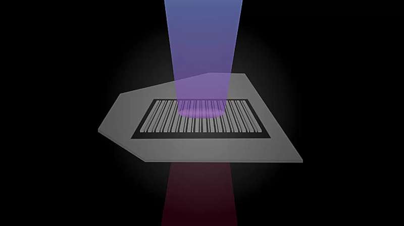
Recent advancements in the field of metasurfaces have opened up exciting prospects for enhancing the performance of electronic devices, particularly in the realm of 2D materials. Researchers have discovered that by etching 2D crystals, they can significantly improve the functionality of these materials, leading to a myriad of applications in modern technology.
The innovative approach involves manipulating the optical properties of these 2D materials through the strategic etching of metasurfaces. This process allows for the fine-tuning of light interactions with the materials, enabling enhanced performance in various devices. The ability to control light at the nanoscale is crucial for advancements in fields such as telecommunications, energy harvesting, and imaging technologies.
One of the key benefits of utilizing etched metasurfaces is the potential for increased efficiency in electronic devices. By improving light absorption and emission properties, these enhanced 2D materials can lead to better performance in photovoltaic cells and other energy-related applications. Furthermore, the integration of these materials into existing technologies can pave the way for more compact and efficient devices, reducing overall energy consumption.
Moreover, the research highlights the versatility of using 2D crystals in combination with metasurfaces. This combination not only provides a pathway to optimize existing technologies but also opens up possibilities for developing entirely new applications, particularly in the area of optoelectronics. The potential for creating innovative devices that leverage the unique properties of these materials is vast, indicating a promising future for technological advancements.
In conclusion, the etching of metasurfaces on 2D crystals represents a significant breakthrough in material science and engineering. This technique not only enhances the properties of these materials but also expands their applicability across various domains. As research continues to evolve in this area, we can expect to see transformative changes in electronic devices that harness the power of nanotechnology and advanced materials.
Please consider supporting this site, it would mean a lot to us!