


TLDR: Recent research reveals that manipulating atomic neighborhoods in semiconductors can significantly enhance their electronic properties, leading to improved performance and energy efficiency. This innovative approach may enable the design of new materials for advanced applications in microelectronics, optoelectronics, and quantum computing, paving the way for future technological advancements.
Recent research has unveiled a groundbreaking approach to the design of microelectronics by exploring the concept of atomic neighborhoods in semiconductors. This innovative perspective could revolutionize how semiconductor devices are engineered, leading to enhanced performance and energy efficiency. The study highlights how the arrangement of atoms within a semiconductor material can significantly influence its electronic properties, thereby opening new pathways for optimizing device functionality.
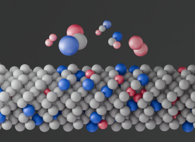
The research focuses on the interactions between individual atoms in semiconductor materials, which can create unique local environments or "neighborhoods." These atomic configurations can alter the behavior of electrons, impacting factors such as conductivity and overall material stability. By understanding and manipulating these atomic neighborhoods, researchers can tailor semiconductors to meet specific requirements for various applications, including microelectronics, optoelectronics, and even quantum computing.
One of the key findings of the study is that small changes in atomic arrangements can lead to substantial changes in electronic properties. This insight paves the way for the development of new materials that can outperform traditional semiconductors. For example, materials that exhibit enhanced charge mobility could be engineered to create faster and more efficient electronic devices. Additionally, this approach may help in reducing energy consumption, a crucial factor in the current technological landscape where sustainability is increasingly prioritized.
The implications of this research extend beyond just improving existing technologies. By leveraging the principles of atomic neighborhoods, researchers can potentially design entirely new classes of semiconductors that can operate under extreme conditions, such as high temperatures or radiation, thus expanding the capabilities of electronic devices in various fields, including aerospace and medical technologies.
As the demand for advanced microelectronics continues to grow, the ability to innovate at the atomic level will be critical. This new understanding of atomic neighborhoods in semiconductors not only provides a fresh perspective on material design but also represents a significant step toward the next generation of semiconductor technology. As research in this area progresses, we can anticipate exciting developments that could transform the landscape of electronics and pave the way for future advancements in technology.
Please consider supporting this site, it would mean a lot to us!